 English
 中文
中文
The cornerstone of chip manufacturing - semiconductor wafer industry overview
2025/4/16 14:30:46
Semiconductor silicon is the semiconductor material with the highest cost ratio and the most critical semiconductor material in the industrial chain. From the perspective of cost ratio, silicon chips accounted for 37% of the market in semiconductor materials, making it the largest semiconductor material. From the perspective of the industrial chain position, silicon wafers, as the starting point of the semiconductor industry chain, directly affect the manufacturing quality of chips. This paper mainly introduces the core semiconductor material silicon wafer and its industry situation in detail.
From the perspective of semiconductor silicon industry chain, the upstream is silicon wafer manufacturers, and the global market is mainly occupied by the leading manufacturers in Japan, Germany, South Korea and Taiwan; Midstream is the wafer processing segment, which is mainly divided into two business models: integrated component manufacturer (IDM) and Foundry. International manufacturers such as Intel, Samsung, Texas Instruments, etc. adopt IDM mode, and its business scope covers all aspects from chip design, wafer manufacturing to sealing and testing. Foundry companies include TSMC, SMIC and so on. Downstream applications of the industry chain mainly involve smart phones, tablets, the Internet of Things, automotive electronics, military space and other fields.
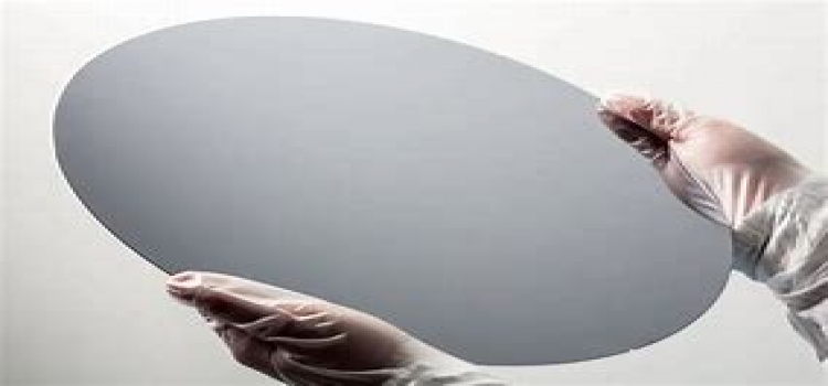
1, the quality control of silicon wafers is strict, and the production technology is difficult
As a semiconductor base substrate, the silicon wafer must have a high standard of purity, surface smoothness, cleanliness and impurity contamination in order to maintain the function of the original design of the chip.
1) Crystal purity and defection-free structure: semiconductor silicon wafer purity requirements of 99.9999999% or more, and the silicon wafer is composed of silicon single crystal arrangement, its structure is similar to diamond, 1 carat diamond is 200 mg, to make a silicon single crystal rod, which is equivalent to making 420 kilograms of diamond structure.
2) Surface cleanliness: the surface particle size is required to reach the nanometer level, and the micro-particles on the silicon wafer used in the advanced process need to be less than 1nm.
3) Surface flatness: the surface height drop is required to be less than 1nm, which is equivalent to the height drop of the field can not be higher than 1 micron within the range of a baseball stadium.
4) No impurity pollution: the surface impurity content is required to be less than one tenth of ten billion, and the parameter control requirements are higher with the advance of the advanced process.
2. Five categories of silicon wafers
1) Polished sheet: After the silicon rod is made, it is cut into slices with a thickness of less than 1mm. After grinding and chemical corrosion, the slices become corrosion sheets. The flatness of the surface of the silicon sheet becomes worse, and surface defects need to be removed by polishing to improve the yield of the chip. Polishing can be directly used to manufacture semiconductor devices, widely used in memory chips and power devices and other fields.
2) epitaxial sheet: the polished sheet is used as the substrate, and a new single crystal layer is grown along the original crystallization direction, and this layer of monocrystalline silicon is the epitaxial layer. Epitaxial chips are commonly used in CMOS circuits, such as general-purpose processor chips (cpus) and graphics processor chips (Gpus).
3) Annealing sheet: the polished sheet is placed in hydrogen or argon, and the heating and cooling process is carried out according to certain procedures to obtain the annealing sheet. Its purpose is to eliminate the effect of oxygen on the resistivity of silicon wafers and improve the chip yield.
4) Silicon on Insulator (SOI silicon) : An oxide layer with high electrical insulation is sandwiched between two polished wafers and then glued together. The bottom plate is thicker and plays a supporting role; The insulation and top layer of silicon are thin, and the circuit is etched on top. SOI silicon wafer has the advantages of low voltage, low power consumption, high integrated density, fast speed, simple process, strong resistance to cosmic ray particles and so on. Therefore, SOI silicon chips are suitable for high pressure, harsh environment resistance, low power consumption, and high integration of chips, such as RF front-end chips, power devices, automotive electronics, sensors, and spaceborne chips.
5) Junction isolation sheet: the polished sheet is designed according to the customer, using lithography, ion implantation and thermal diffusion technology to form an embedded layer of integrated circuit on the surface of the wafer, and then forming an epitaxial layer on the top of the layer.
3. Silicon wafers continue to develop in the direction of large sizes
At present, the world's mainstream silicon wafer size is 12 inches and 8 inches, according to Gartner data, according to the global output value, 12 inches of silicon wafer production capacity accounted for 64%, 8 inches accounted for 28%. Silicon wafer commonly used sizes include 4, 6, 8, 12 inches; Among them, semiconductors mainly use 8-inch and 12-inch large silicon wafers. Under the same process conditions, the utilization rate of 12-inch silicon wafers is 2.25 times that of 8-inch silicon wafers, and 12-inch large silicon wafers have become the main development trend in the future.
4. Silicon wafers are widely used in downstream applications
1) 12-inch silicon wafers are usually used for advanced integrated circuit manufacturing processes below 90nm: involving high-end fields such as logic chips (CPU, GPU), memory chips, FPgas and ASics. The market demand has benefited from the technological upgrading of terminal semiconductor products such as smartphones, computers, cloud computing, and artificial intelligence.
2) 8-inch silicon wafers are usually used for characteristic processes above 90nm to microns: involving power devices, power managers, MEMS, display drivers and fingerprint recognition chips. In the future, the market demand for applications such as the Internet of Things and automotive electronics will increase, and the market scale will continue to expand.
3) 6-inch silicon wafers are usually used in 0.35-1.2 micron processes: involving power devices, discrete devices and other fields.
5, the global silicon market competition pattern
1) Monopoly of international manufacturers and high industry concentration
According to SEMI data, the world's top five silicon wafer manufacturers (CR5) market share is as high as 92%. Among them, Japan's Shin-etsu Chemical market share of 28%, the world's largest silicon chip manufacturer; Japan's SUMCO ranks second with 24 per cent; The remaining manufacturers are Taiwan Global Wafer of China, Silitronic of Germany, and SK Siltron of South Korea. From China's point of view, the domestic silicon wafer manufacturers mainly include Zhonghuan shares and silicon Industry Group, the market share of the two enterprises is about 3%, which is relatively low in the global market. Strict quality management, technical standards, and long-term customer verification will become the key for wafer manufacturers to compete in the silicon industry.
2) China's wafer production capacity continues to increase, promoting the development of silicon wafer manufacturing industry
According to SEMI data, from 2017 to 2020, the Chinese mainland will account for 42% of the world's new fabs. Beginning in 2020 With the gradual completion of construction, the fab began to enter the stage of trial production to expansion. In the next five years, China's wafer production capacity will usher in a rapid increase. Under the background of the third semiconductor industry transfer in the world and the Chinese mainland becoming a semiconductor manufacturing center, China's local silicon wafer manufacturers will usher in a period of leapfrog development.
- PRE: Mirror polishing technology, too complete!
- NEXT: 没有了